PCB Design For IoT Development: How Good Prototyping Can Help You Avoid Costs
Key Takeaways
- Early prototyping saves significant money: An inexpensive prototype, costing as little as $5-$20, can reveal critical design flaws that would otherwise cost thousands to fix in later development stages
- Smart design strategies deliver substantial manufacturing savings: Minimizing board size and layer count can lead to 15-25% cost reductions through simplified routing and reduced via count
- Custom IoT PCBs provide 50-70% unit cost reductions at scale while shorter development cycles provide competitive advantages through earlier market entry
- Proper prototyping can significantly reduce the high failure rate that plagues IoT projects in proof-of-concept stages, which is reported to be around 30% by some studies
- Expert PCB design partners maximize cost savings through proven methodologies and industry experience
IoT product development often faces significant challenges, with many projects experiencing timeline delays and budget overruns. While specific averages vary, some reports indicate average IoT projects costing around $556,000. However, companies that invest in effective PCB prototyping early in the development process consistently avoid these costly pitfalls while delivering superior products faster.
IoT Project Failures: How Poor PCB Design Creates Massive Financial Losses
The statistics paint a sobering picture of IoT development challenges. Nearly one-third of IoT projects fail during the proof-of-concept stage, often because implementation costs spiral out of control or the bottom-line benefits become unclear. Large-scale IoT initiatives frequently exceed budgets by 45% while delivering significantly less value than promised to stakeholders.
Poor PCB design lies at the heart of many project failures. Layout issues, power management problems, or component selection errors that surface late in development create financial impacts that cascade through every subsequent phase. Manufacturing delays, field failures, and expensive redesigns transform what should be profitable products into costly lessons.
The ripple effects extend beyond immediate costs. Market launch delays allow competitors to capture market share, while product recalls damage brand reputation and customer trust. Companies that skip proper prototyping phases often discover critical flaws only after investing heavily in tooling and initial production runs.
Why IoT PCB Prototyping Prevents Expensive Hardware Failures
1. Catching Layout Issues Before They Become Thousand-Dollar Problems
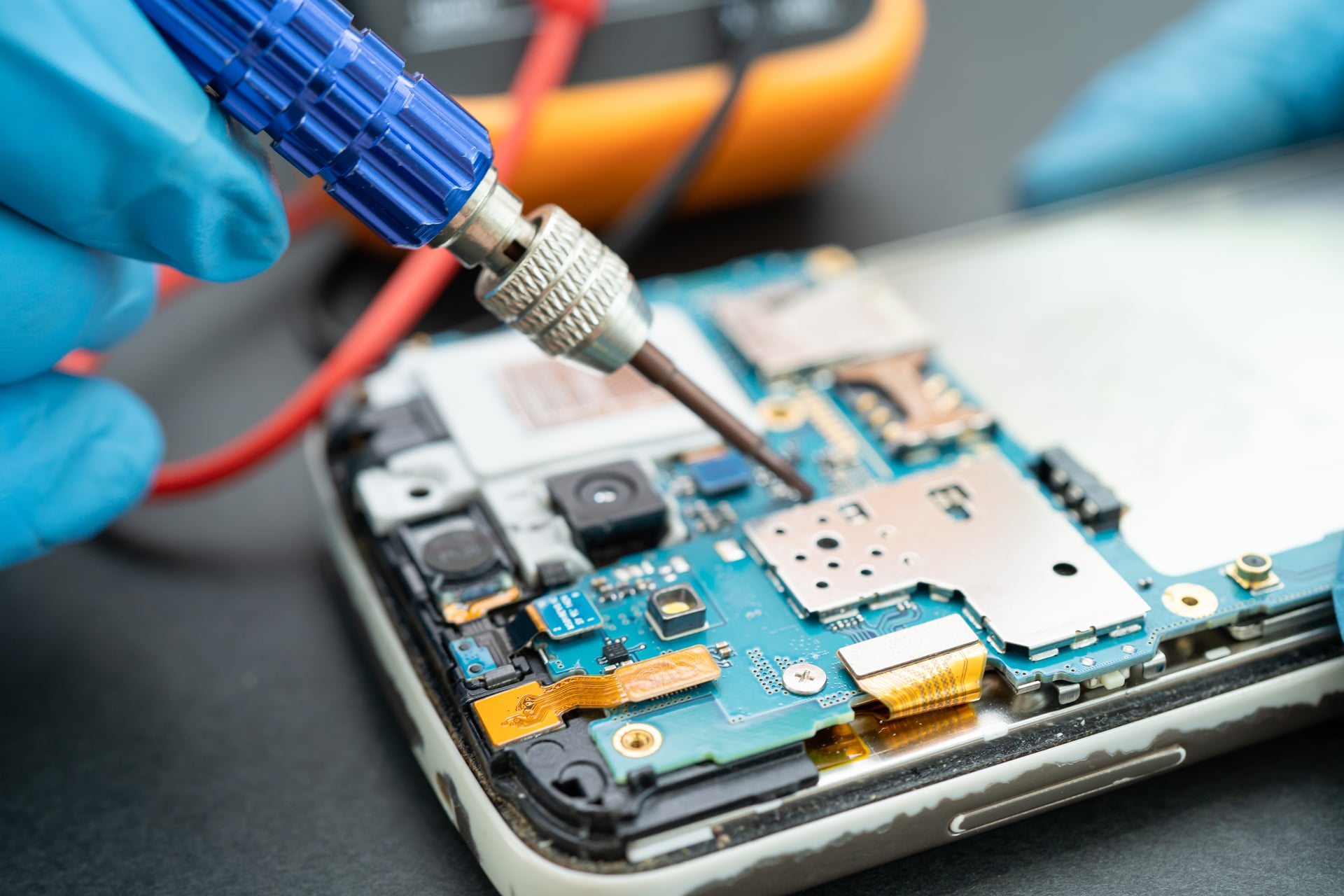
Consider an example where an investment of just $10 in a simple 2-layer PCB prototype could reveal a critical layout issue, potentially saving thousands in rework costs in later development stages. The prototype caught trace routing problems, component placement conflicts, and signal integrity issues that would have been catastrophically expensive to address during production.
Layout problems multiply costs geometrically as projects advance. What costs dollars to fix in prototyping becomes hundreds of dollars during design validation, thousands during tooling, and tens of thousands after production begins. Expert PCB design services like those available from Rabbit Product Design use proven methodologies to identify and resolve these issues during the most cost-effective phase of development.
2. Power Management Testing Extends Battery Life and Reduces Maintenance
Battery life directly impacts user satisfaction and long-term maintenance costs for IoT devices. Prototyping reveals power consumption patterns under real-world conditions, allowing designers to optimize power management circuits before finalizing designs. Efficient PCB design can extend battery life significantly, reducing the frequency of battery replacements and associated service costs.
Power distribution network optimization during prototyping prevents voltage regulation problems that could cause device malfunctions or premature component failures. Testing different power management strategies early in development helps identify the most efficient approaches for specific IoT applications, whether they require always-on sensing or intermittent data transmission.
3. Component Selection Validation Prevents Market Launch Delays
Poorly selected components create functional failures that increase testing time, complicate diagnosis, and ultimately raise the costs of bringing products to market. Prototyping validates component choices under actual operating conditions, revealing performance limitations or compatibility issues before they impact production schedules.
Component availability and supply chain stability also become clear during prototyping phases. Discovering that a critical component has long lead times or limited availability early in development allows time to identify alternatives without delaying market launch. This proactive approach prevents the costly scramble to find substitute components after production has already begun.
Smart Design Strategies That Cut PCB Costs by 15-25%
1. Minimize Board Size and Layer Count for Maximum Savings
Two-layer PCBs can be significantly less expensive to manufacture than multilayer boards, with some basic 2-layer IoT PCBs costing as little as $0.50-$2.50 per unit, compared to $15-$25 or more for complex 6-layer HDI PCBs. Smaller board dimensions can lead to substantial reductions in material and fabrication costs, with techniques like integrating vias into pads potentially reducing the overall PCB footprint by up to 30-40%.
Compact designs also reduce material costs and improve manufacturing yield rates. However, minimization requires careful balancing of electrical performance, thermal management, and manufacturing constraints. Experienced designers know how to achieve maximum space efficiency while maintaining signal integrity and meeting regulatory requirements.
2. Optimize Power Distribution Networks for Custom IoT Applications
Power distribution network optimization reduces both manufacturing costs and operational expenses. Well-designed power delivery systems require fewer components, simplify assembly processes, and improve overall system reliability. Custom power management solutions eliminate unnecessary features while focusing resources on application-specific requirements.
Optimized power networks also reduce electromagnetic interference, potentially eliminating the need for expensive shielding solutions. This dual benefit of cost reduction and performance improvement makes power distribution optimization a high-priority design consideration for cost-conscious IoT projects.
3. Use Simulation Tools to Eliminate Signal Integrity Problems
Advanced simulation tools identify signal integrity problems before physical prototypes are built, reducing the number of design iterations required. Time-domain reflection analysis, crosstalk analysis, and voltage drop analysis help optimize designs for reliable performance while minimizing component requirements.
Simulation-driven design reduces prototype costs and accelerates development timelines. By identifying and resolving potential issues in software, designers can focus physical prototyping efforts on validating optimized designs rather than troubleshooting fundamental problems.
Real Cost Analysis: What Early Prototyping Actually Saves
Development Cycle Improvements Reduce Overall Project Costs
Organizations implementing effective prototyping strategies often report shorter development cycles, accelerating time-to-market. Shorter development cycles also provide competitive advantages by enabling earlier market entry. First-mover benefits in rapidly evolving IoT markets can significantly exceed the direct cost savings from efficient development processes. Companies that consistently deliver products faster than competitors capture larger market shares and command premium pricing.
Custom PCBs Deliver 50-70% Unit Cost Reductions at Scale
Custom IoT PCBs enable 50-80% unit cost reductions for large production volumes by allowing selection of only necessary components. This optimization helps offset initial non-recurring engineering costs while providing long-term manufacturing advantages. Custom designs eliminate features that generic boards include but specific applications don't require.
The break-even point for custom PCB development typically occurs between 1,000 and 10,000 units, depending on design complexity and feature requirements. Beyond this threshold, cost savings compound with each additional unit produced, making custom designs increasingly attractive for successful IoT products.
Essential Prototyping Techniques for Compact IoT Devices
1. Multilayer PCB Design for Space-Constrained Applications
Multilayer PCBs enable high-density component placement while providing dedicated layers for power distribution and ground planes. This approach reduces board size while improving electromagnetic interference shielding and signal integrity. Advanced stack-up configurations allow integration of mixed-signal and RF circuits on the same board.
Layer planning during prototyping reveals optimal configurations for specific applications. Testing different stack-up approaches helps identify the minimum layer count required for reliable performance, balancing functionality with manufacturing costs.
2. Thermal Management Strategies for High-Performance IoT
Thermal management becomes critical as IoT devices incorporate more processing power in smaller form factors. Prototyping reveals heat distribution patterns and validates thermal management solutions before committing to final designs. Thermal vias, copper pours, and strategic component placement help dissipate heat effectively.
Temperature-sensitive components require particular attention during thermal design validation. Prototyping under various operating conditions ensures that microcontrollers, RF transceivers, and power management circuits remain within safe operating ranges throughout the device's operational envelope.
3. EMI Shielding and Grounding for Wireless Communication Reliability
Proper grounding and electromagnetic interference shielding are essential for reliable wireless communication in compact IoT devices. Ground plane implementation, differential signaling techniques, and strategic shielding placement prevent interference while maintaining signal quality. A logistics company successfully used custom IoT sensors with rigid-flex PCBs to monitor temperature and humidity during shipping, resulting in reduced spoilage and lower operational costs.
Prototyping validates EMI mitigation strategies under real-world conditions. Testing in electromagnetically noisy environments helps identify potential interference sources and validates shielding effectiveness before production begins. This validation prevents costly redesigns after products fail regulatory testing.
Partner with Expert PCB Designers to Maximize Your Cost Savings
Experienced PCB design partners bring proven methodologies, advanced tools, and industry expertise that individual companies rarely possess internally. They understand the subtle trade-offs between cost, performance, and manufacturability that determine project success. Expert designers also maintain relationships with component suppliers and manufacturing partners that can provide cost advantages and supply chain stability.
The right design partnership accelerates development timelines while reducing risks. Experienced teams have encountered and solved similar challenges across multiple projects, allowing them to anticipate potential issues and implement preventive measures. This expertise translates directly into cost savings through reduced development iterations and faster time-to-market.
Collaboration with expert PCB designers also provides access to cutting-edge design tools and simulation capabilities that might be prohibitively expensive for individual companies to license and maintain. These tools enable more sophisticated optimization and validation, leading to better products at lower total costs.
For IoT product development managers seeking to avoid the costly pitfalls that plague 75% of projects, partnering with a reputable design consulting firm provides the expertise and proven methodologies needed to deliver successful IoT products on time and within budget.
Rabbit Product Design
City: Palo Alto
Address: 2100 Geng Rd Ste 210
Website: https://www.rabbitproductdesign.com/


Comments
Post a Comment